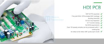
HDI Printed Circuit Board Manufacturing Challenges
HDI Printed Circuit Board
Compared to traditional PCBs, HDI PCBs have fewer vias (electrical connections between different layers of the board), pads (the metal on which components are soldered), and traces (the paths electrical signals travel through). This allows them to be smaller, lighter, more reliable, and have better performance power. Additionally, they require fewer materials and offer faster prototyping lead times.
Despite the many benefits of HDI PCBs, they can be challenging to manufacture. Intricate manufacturing processes, such as laser drilling and multiple lamination cycles, can increase the cost of HDI PCBs compared to standard PCBs. These higher costs can have a direct impact on product development timelines and the time it takes for electronic devices to reach market.
The HDI PCB manufacturing process is complex and requires a high level of technical expertise and the latest state-of-the-art equipment for precise manufacturing. These processes also require clean room environments to maintain proper process control and reduce defects. The fabrication of HDI PCBs with ultra-fine lines, tight spacing, and annular rings is especially challenging. In addition, HDI PCBs are typically plated using an immersion reflow process that requires precise temperature control.
HDI Printed Circuit Board Manufacturing Challenges
In addition to these challenges, there are several other factors that can impact the success of an hdi printed circuit board. For example, proper thermal management is critical to avoid overheating, which can damage components and impede signal flow. Likewise, a poor fanout strategy can result in shortened life-cycles and increased maintenance costs.
One of the key features distinguishing HDI circuit boards is their use of microvias. Microvias are tiny holes drilled into the substrate of the circuit board, typically with diameters measuring in micrometers. These microvias serve as conduits for routing signals between different layers of the board, effectively increasing the available routing density without expanding the board’s physical dimensions. By utilizing microvias, HDI circuit boards can achieve greater levels of integration and functionality, making them ideal for applications where space is limited and performance is critical.
It’s also important to design your HDI circuit boards for manufacturability. This includes ensuring that the layer stack-up meets manufacturer guidelines, and considering factors like core materials, prepreg thicknesses, and the location of ground and supply planes. It’s also essential to ensure that silkscreen and reference designators are properly placed and legible.
Lastly, you must consider signal integrity. This involves minimizing impedance discontinuities between traces and the reference plane, as well as reducing crosstalk between signals. To minimize these issues, it’s best to use a solid ground plane beneath and in between high-speed signal layers. It’s also important to route traces over a via or a void in the reference plane rather than through it, as this can cause signal degradation.
In addition to these tips, it’s also a good idea to use narrower trace widths to improve routing density and minimize the number of vias in your circuit board. Narrow trace widths also help to limit the effects of inductive coupling, a phenomenon that occurs when a magnetic field induces voltages in nearby loops of wire that are close in size and direction. This is due to the fact that the current in these loops creates a magnetic field that acts as an antenna and can pick up interference from other signals.